
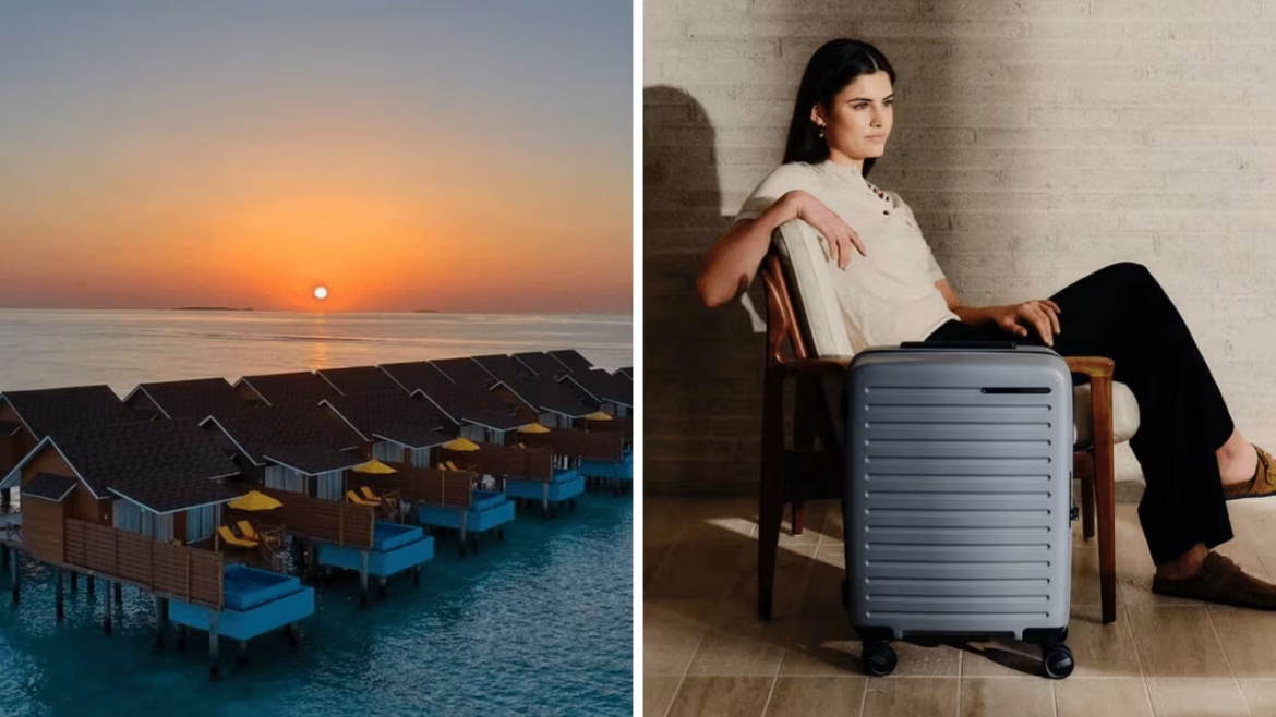
We’ve made it. The End of Financial Year (EOFY) sales are officially here, and our favourite travel brands are not here to play.
And since every brand under the sun has been bombarding us with EOFY emails since the start of the month, it’s easy to feel overwhelmed.
That’s where we come in. We’ve sifted through thousands (and we mean thousands) of travel deals – from a 66 per cent off an all-inclusive dream Dhigufaru Island Maldives Paradise holiday with Luxury Escapes (flights included) to saving $400 on a brand spanking new Samsung S26 Ultra that you can take all your travel pics on – to find the best ones that are actually worth shopping.
I’ve been covering EOFY sales for years, and my biggest tip is this: Always start with your big-ticket, investment buys first – think a Samsonite suitcase that you’ll be using for years to come, or a honeymoon holiday you’ve been meaning to finally book – because there’s no better time than now to seal the deal. And also don’t forget the ‘boring’ things like a Ubigi travel eSIM to make your next trip easy (your future self will thank you).
Starting with travel essentials – I can’t go anywhere without my Sony WH-1000XM5 noise-cancelling headphones. Popping them on instantly cancels out all the cabin noise when flying, and it’s honestly pure bliss. It’s only $418 (down from $445) at The Good Guys.
Another great pick that frequent travellers love is the Bose QuietComfort Headphones, which are currently 45 per cent off at Myer for $299. And since we’ve been covering EOFY sales every year, this is actually the lowest price Myer has had them during EOFY – they’re $30.95 cheaper now than they were in Myer’s EOFY sale last year (yes, we’ve been keeping tabs).
Staying in line with travel tech, you can upgrade your laptop with HP’s EOFY sale on their best-selling range of HP Chromebooks or get $300 off this HP 14-inch Laptop – you can even score an extra 10 per cent off with the code ‘EOFY’. Or perhaps you’re more of an Apple fiend; the Apple MacBook Pro 14-inch with M5 Chip (1TB/24GB) is currently $202 off at JB Hi-Fi.
Whether you’re mysteriously tapping away in the airport lounge or you’re living your best digital nomad life, now’s the perfect time for a cheeky tech upgrade.
As for travel beauty essentials, look no further than Dyson. The oh-so-coveted Dyson Airwrap i.d. Multistyler and Dryer is $252 off, and you’ll even get a free detangling comb, hair clips, and a bottle of Chitiosan Pre-style cream (worth $134 all up). Salon-worthy blow-outs while sipping a cocktail somewhere tropical just got a whole lot real.
If you’re travelling with a little one, a travel-friendly pram is a must. Milly + Coup’s Pixi Travel Stroller is currently $100 off. It’s super lightweight at only 6.5kg altogether and comes with a carry bag, belly bar, and stay-put harness covers. Many reviewers praise it for its build quality and lightweight design that’s “easy to fold with one hand”.
It’s a “must-have for easy plane travel,” notes a five-star reviewer.
Looking for something more niche? Our favourite online marketplace, eBay, has all the travel bits and bobs you never knew you needed – like a handy tech organiser that’s under $10 or a set of compression packing cubes to fit all your travel ‘fits without a worry.
To ensure you’re comfy in flight, Trtl has shaved 30 per cent off bundles, the ‘Rolls-Royce’ of travel neck pillows – the Cabeau Evolution S3 – is also a whopping 41 per cent off on Amazon, while The Oodie has recently dropped the cosiest sherpa-lined hoodies – which are all on sale, too. Boody’s Feel Good Sale offers up to 50 per cent off best-selling underwear, socks, PJS, and more (basically everything that’s comfy).
Moving on to luggage. Luckily for you, I don’t think there’s a big-name brand that hasn’t already dropped a sale. We’ve got up to 50 per cent off at Samsonite, Antler, American Tourister and Bagsmart. Shoppers can also snag 30-40 per cent off High Sierra, and up to 10 per cent off Monos. For our favourites over at July, they’re running a classic ‘Bundle & Save’ deal, where you can save up to $240 if you purchase two products with a combined value of $1,200 – great if you’re planning to upgrade your entire set.
Retailers have also joined in the fun with Strand taking up to 50 per cent off luggage and handbags, and Myer dropping their tried-and-true 40 per cent off luggage deal.
With your cases and clothing sorted, it’s time to book that well-deserved holiday.
Inspiring Vacations is doing a 40 per cent off select tours. From a small group tour through the rolling hills of South America to a 21-day African safari tour through Cape Town, the savings are huge.
My Cruises has not held back with its last-minute cruise sale, where you can get a further, yes, further, $1000 off already heavily discounted last-minute tours. And of course, Luxury Escapes can do us no wrong, with exclusive holiday packages to the Maldives, such as 67 per cent off the Meyyafushi Maldives and Flights hotel-and-flight bundle. Did someone say all-inclusive pool villas and free-flowing drinks? Count us in.
And when you’re done with galivanting around the world, heading home to a comfy bed and an easy daily routine makes all the difference. Upgrade your bed with Amart’s EOFY sale – they’re slashing 20 to 60 per cent off everything. We have our eyes on the limited-edition Trinell Queen Bed, which is currently $1,100 off.
For our Pilates Princesses, Your Reformer is making it simple to stay fit between trips. Either rent a reformer machine for $39 per week and work out on your own schedule at home (not a studio), or set up your home gym with your very own starting at $2995 – while the initial cost may seem big, you’ll ‘pay it off’ in no time, considering a single Pilates class can be anywhere from $35 to $50+ a class.
If you’ve been clutching your credit cards, waiting for the final moment to shop the EOFY sales, take this as your sign to shop now. You’ve done it – you’ve waited it out to see all the best deals trickle through without caving in. Our advice? Don’t wait any longer. Most EOFY sales have dropped, and with jaw-dropping sales come demand – and many tours, flights, cruises and travel must-haves sell out fast. Wait too long, and you’ll miss the boat (literally).
Read on for our hand-picked list of the best EOFY sales and discounts you can shop right now.
Jump to:
Please note: Prices are correct and products are in stock at the time of publishing. We’ll do our best to keep this story updated, but be aware products move fast during sales events.
EDITOR’S PICKS: What are the best EOFY deals overall?
Luxury Escapes
Inspiring Vacations
Samsonite
Samsung
My Cruises
Paire
Milly + Coup
Boody
Simplify Living
Amazon Australia
David Jones
Myer
The Iconic
American Tourister
High Sierra
Antler
Wendy Wu
The Oodie
Ubigi
The Good Guys
Amart
HP
eBay
Dyson
- Save $252 on the Dyson Airwrap i.d. multi-styler, $597 (down from $849). Includes free detangling comb, hair clips, and Chitosan Pre-style cream, worth $134.
- Save $255 on the Dyson Airstrait straightener and dryer, $494 (down from $749). Includes free paddle brush and Chitosan Pre-style cream, worth $109.
- Save $300 on the Dyson Supersonic Nural hair dryer, $449 (down from $749). Includes a free detangling comb worth $25.
- Save $202 on the Dyson Supersonic r hair dryer – Straight+Wavy, $597 (down from $799). Includes free vented barrel brush and Chitosan Post-style serum, worth $109.
- Save $400 on the Dyson V15 Detect™ Absolute vacuum + Dok, $899 (down from $1,299)
Your Reformer
What are the best EOFY travel deals?
Flight Centre
Mix & Match
Etihad Airways
Qatar Airways
Celebrity Cruises
Booking.com
Hilton
Pan Pacific Perth
Skyscanner
G Adventures
Trip.com
What are the best EOFY travel accessories deals?
Trtl
Zorali
Nordace
Strand
Monos
Bagsmart
Anaconda
Zoomlite
What are the best EOFY tech deals?
JB Hi-Fi
Lenovo
What are the best EOFY Beauty & fashion deals?
Boody
Paire
Blue Illusion
The Iconic
Country Road
Under Armor
Oroton
Adidas
Oz Hair and Beauty
Lovehoney
Ugg Express
What are the best EOFY home deals?
Circa
Sheridan
Sheridan Outlet
FREQUENTLY ASKED QUESTIONS ABOUT THE END OF FINANCIAL YEAR SALES
What are End of Financial Year sales?
The End of Financial Year Sale, also known as EOFYS, Mid-Year Sale and Stocktake Sale, is one of the biggest sales events of the year. It typically runs throughout June, concluding on June 30.
How long do the End of Financial Year sales last?
The End of Financial Year sales run until June 30, which is the end of the tax year.
What products are on sale during the End of Financial Year sales?
What once was a way for stores to move stock before the end of the tax year, the End of Financial Year Sales has since grown to encompass all manner of categories – including travel. While whitegoods and homewares are often heavily discounted, during the sales you’ll also find fantastic deals across flights, accommodation, tech, fashion and beauty, too.
See more:
